Photonics
Photonics is the science that focuses on the interaction between light and matter, and on the technologies that enable its generation, transmission, detection and control. It enables innovative solutions across a wide range of industrial, medical and scientific applications. HEF Photonics combines expertise in precision optics, specialty glass, photolithography and advanced optical coatings to support customers from R&D to volume production.
Contact our experts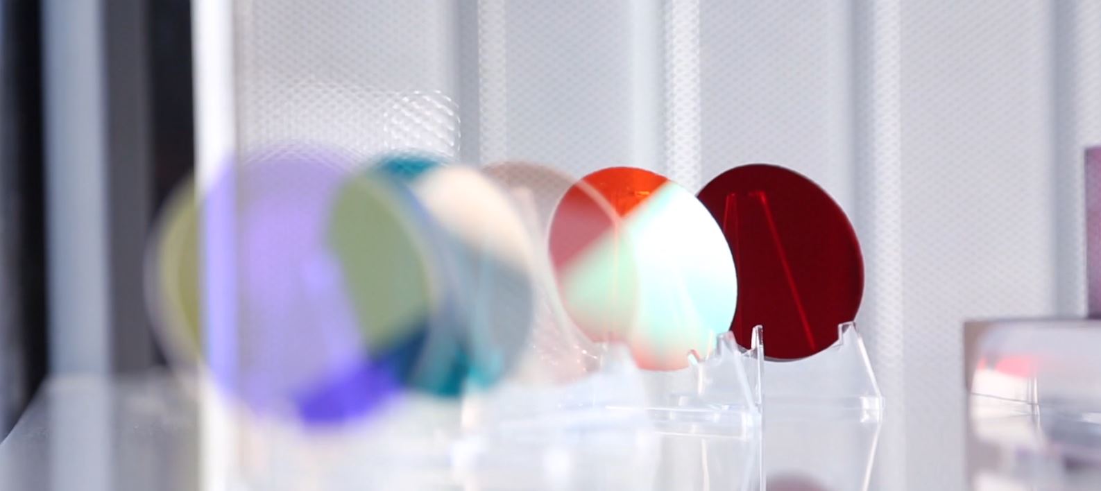
Light on a technology of the future
Electronics is based on the control of electrons, while photonics focuses on the generation, propagation and detection of light using photons – the elementary particles of light first described by Albert Einstein at the beginning of the 20th century.
Optics studies the propagation of light through different media such as air, glass and vacuum. For centuries, it has been the source of major innovations, from telescopes and microscopes to everyday optical devices such as glasses and camera lenses.
Building on these principles, photonics goes one step further by enabling light to be generated, manipulated and detected with exceptional precision, paving the way for advanced solutions for today’s industrial, scientific and medical applications.
From prototype to production – our expertise at the service of your industry
HEF Photonics brings together complementary technologies covering the entire photonics value chain, from specialty glass and precision optics to photolithography and advanced optical coatings.
Precision polishing:
- Precision up to λ / 20 for diameters below 300 mm
- Materials: silica, sapphire, silicon, germanium, ceramics, quartz, Zerodur…
- Shapes: windows, mirrors, prisms, lenses, waveplates, filters…
- Polishing of components up to 1000 mm
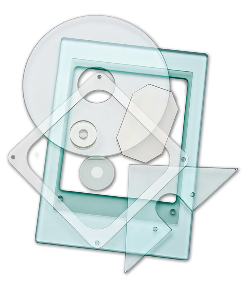
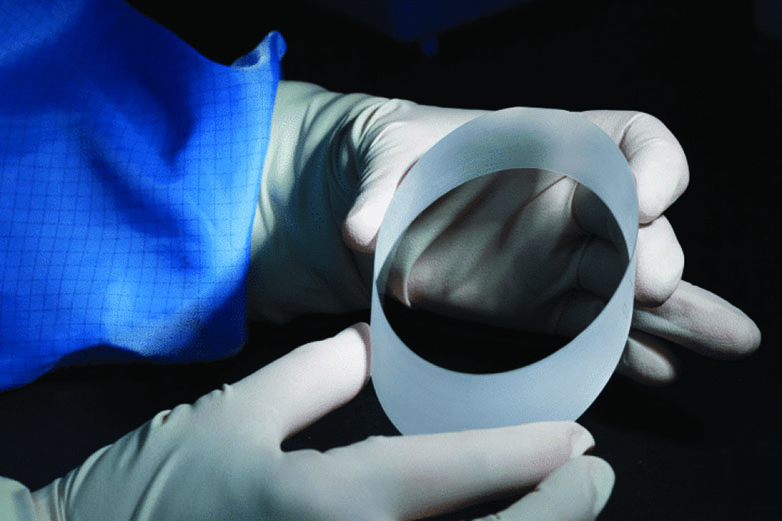
Glass manufacturing technologies:
- Specialty glass and chemically etched glass
- Chemical strengthening and thermal tempering
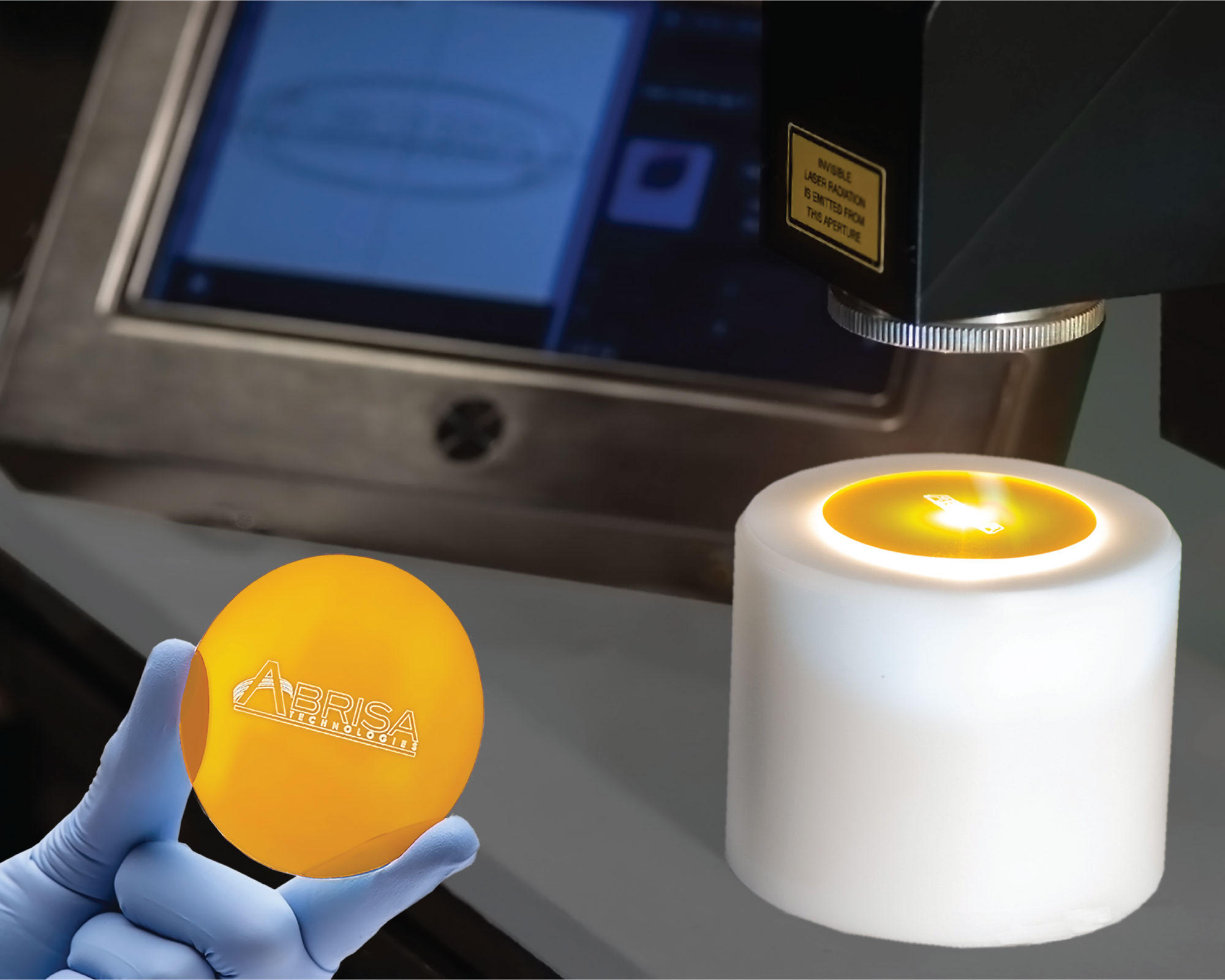
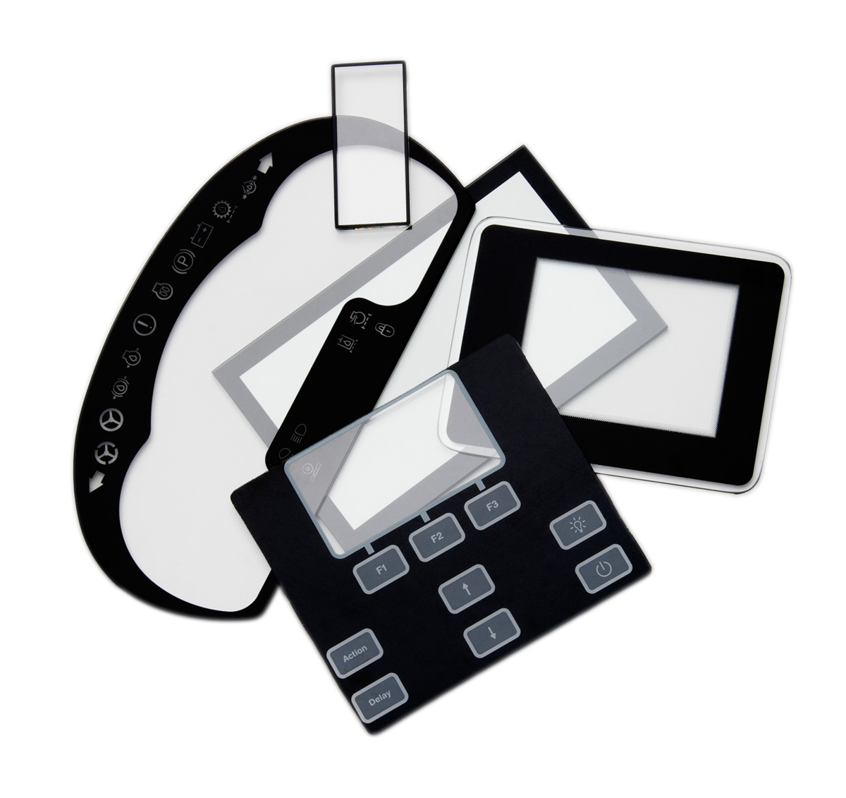
- Screen printing and laser marking
- Ready-to-integrate assemblies
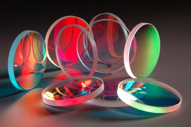
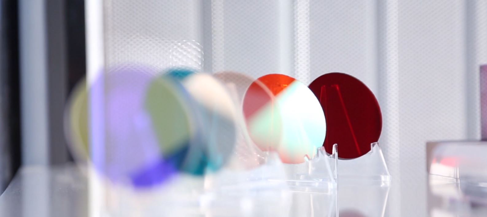
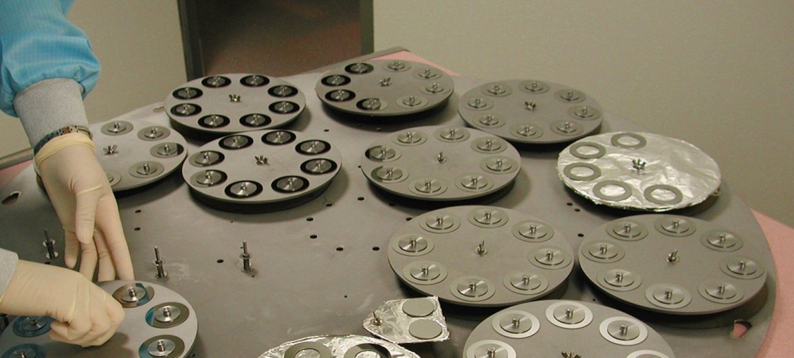
Optical thin-film coatings:
More than 50 deposition chambers dedicated to the production of high-precision optical coatings.
Technologies: electron beam deposition, ion-assisted deposition (IAD), sputtering, ion beam sputtering (IBS), evaporation and thermal CVD for high-precision optical applications.
Applications and capabilities:
Wavelength range: from 200 nm (UV) to 20 µm (far infrared).
Coating solutions are available for glass, crystals, chalcogenide materials, semiconductors, metals and polymer optics, addressing a wide range of optical applications.
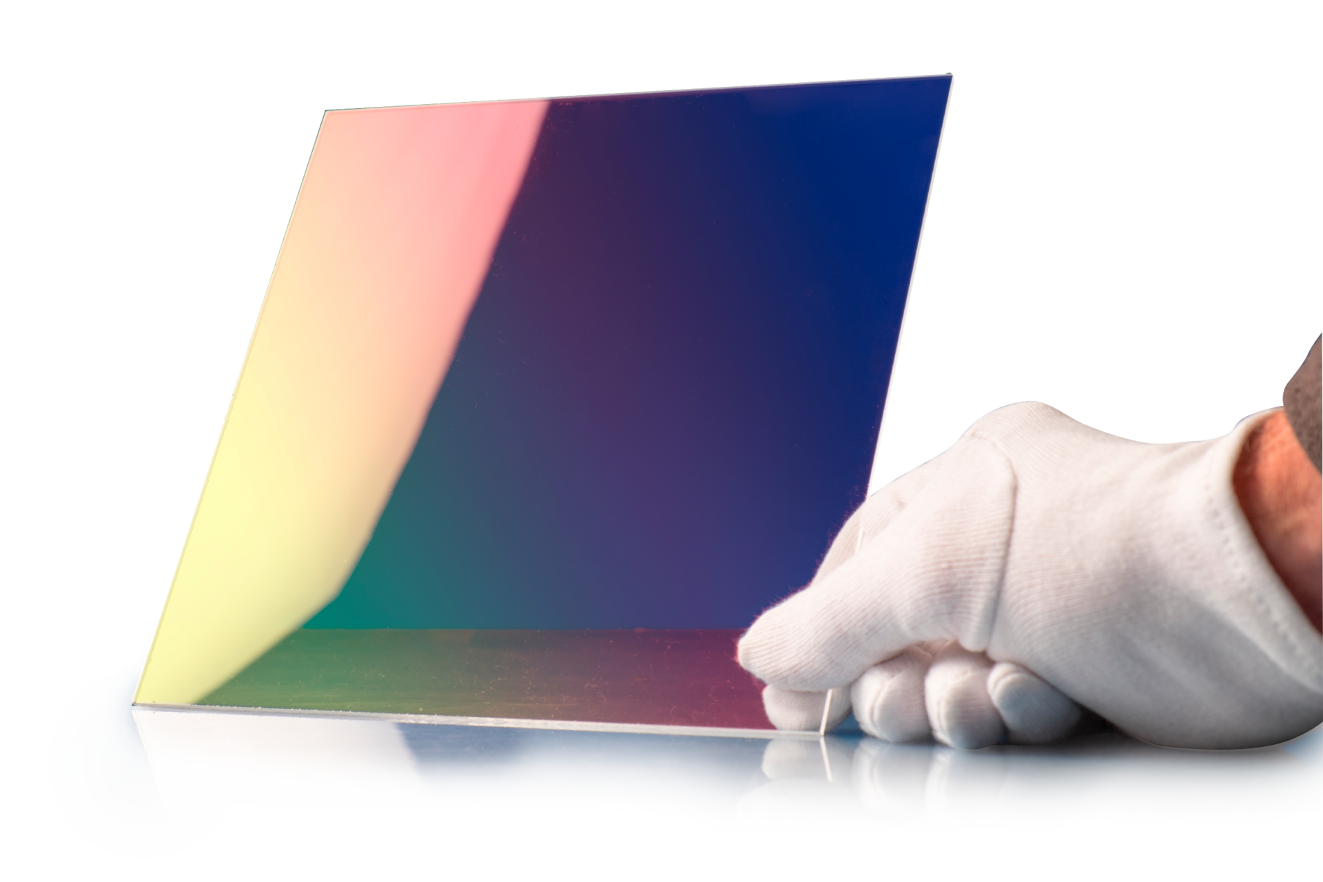
Our portfolio includes advanced optical coatings, such as high-performance mirrors, precision optical filters, beam splitters and custom multilayer coatings for the most demanding photonics applications.
- Anti-reflective, metallic and dielectric coatings
- Polarizing coatings
- Internal (prism) or external coatings
- Deep-black absorbing coatings
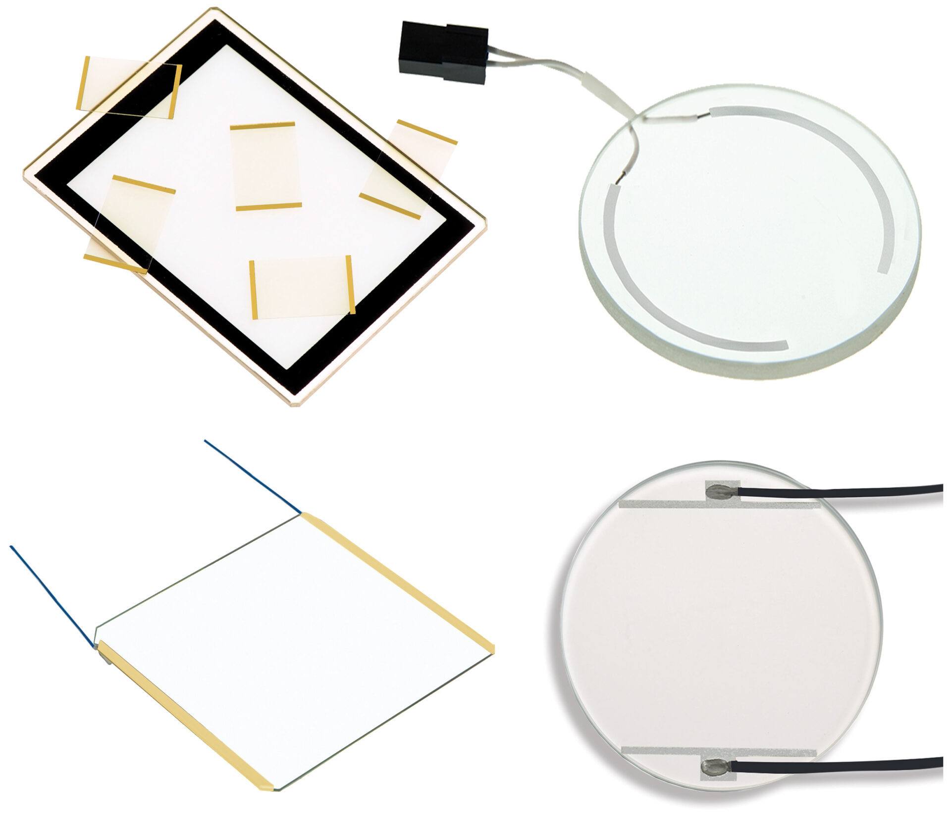
- Transparent conductive coatings (ITO / IMITO)
- Bus bars
- Hydrophobic coatings
- High laser damage threshold coatings
- Environmental resistance tailored to customer requirements; in some cases, a compromise is necessary between resistance to harsh environments and high optical performance

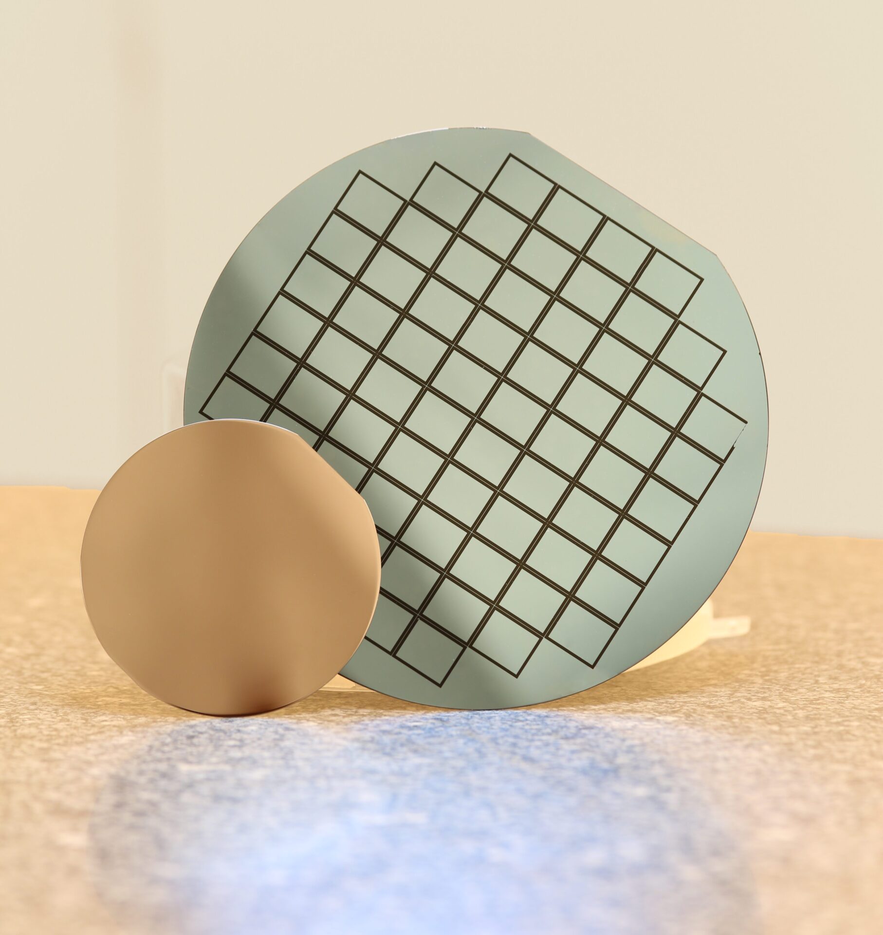
Masking and lithography:
Patterning technologies including photolithography, lift-off, wet etching and laser processing:
- Masking and creating complete optical components
- On 2” to 8” substrates.
- Resolution down to 1 μm in width and 0.15 μm in thickness
- Different types of substrates and etched materials (Al, Ag, Cr, Cu, Ni, Au, etc.).
Electroforming:
- Nickel deposition, thickness from 30 to 200 μm
- Circles, pits, closed shapes down to the micron
- Coatings for emission control and reflection control
Precision cutting:
Technologies: laser, die-cutting, waterjet, slicer, wafer cutting:
- Glass, specialty glass, Si wafers, metals, polymers and batteries
- Thickness up to 0.05 mm
- Lateral smoothness up to 3 μm
- CNC machining
New uses for LED light
Photonics is involved in new uses for interaction with everyday objects.
This interaction will be accomplished by the presence of either tactile screens or non-tactile screens. This interaction can also occur by means of opto-electronic devices that track eye movement – if the pointing function is not done by the hand.
HEF is also active in this field and develops screens for an extensive range of applications that extends from screens for video games to tactile controls used by pilots of the Rafale combat aircraft or future projects involving connected autonomous vehicles.

HEF PHOTONICS: A Global Photonics Network
HEF Photonics brings together complementary expertise in precision optics, specialty glass, photolithography, optical coatings and industrial manufacturing. By combining these capabilities within one integrated network, we support customers from prototype development to high-volume production.
Learn about the production sites of our subsidiaries: