HEF offers advanced surface engineering technology for demanding applications: ultra-fast laser treatment, physical vapor deposition (PVD) coating for electronics, and photolithography, on cutting-edge equipment for prototyping or industrial production.
There are infinite possibilities for creating innovative effects with fast treatment times and high precision.
Our laser platforms work on:
- TGV (Through Glass Vias) and high-aspect ratio interposers;
- wafer cutting; and
- creating microchannels, as well as 3D decorating
with micron-order precision on any type of material (glass, ceramics, polymers, composites, metals, etc.).
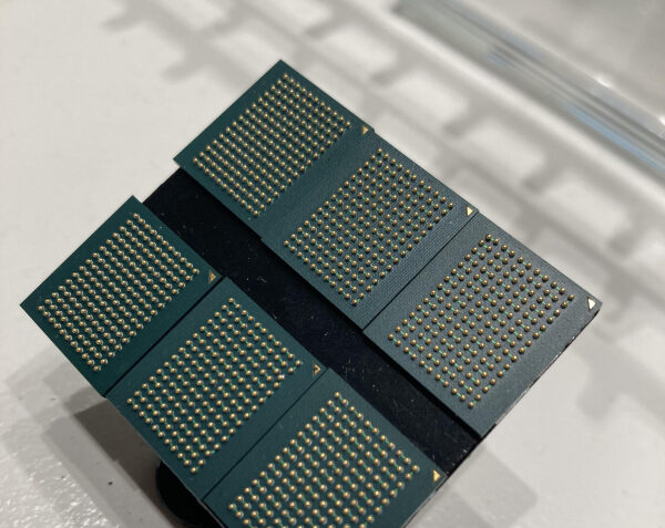
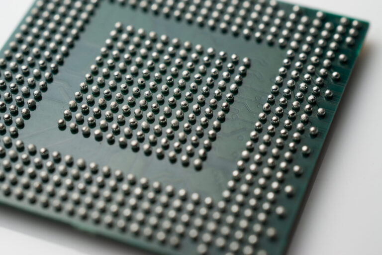
HEF is player in the electronics packaging market thanks to a collaborative project initiated by Thales. In this project, HEF develops solder balls with a polymer core, called “Superballs”. This unique technology makes it possible to better absorb thermo-mechanical variations of PCBs. This ensures optimal spacing between the components and the printed circuit in harsh environments and offers an alternative to lead solder balls.