Everything you need to know about ultra-fast laser surface treatments
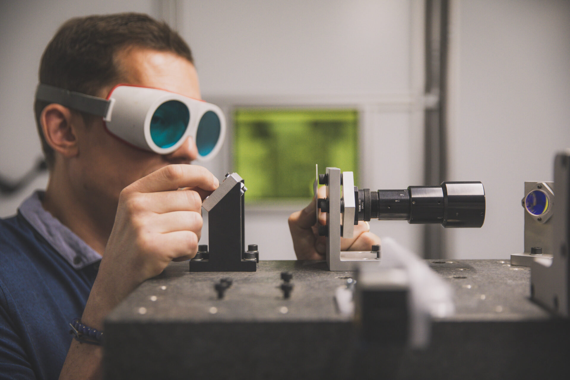
Ultra-fast laser processing (femtosecond laser) enables functionalization, texturing, or micromachining through rapid processing without damaging the material, on a large range of 2D or 3D materials.

What are the advantages of femtosecond lasers?
A Femtosecond laser (or ultra-fast laser) is a surface treatment technology that uses ultrashort optical pulses to engrave, texture, cut, or functionalize any type of material without causing thermal damage.
Technical characteristics of our femtosecond laser processes:
- Works on any material, from the strongest to the most fragile
- Extreme precision
- Thermal control
- No pre-treatment or post-treatment
- Reproductibility
- Wide range of surface geometries: flat 2D or complex 3D
- Any component size from μm² to m²
- Material removal without burrs or thermal impact
- Dimensional control
Operational benefits of our ultra-fast laser technologies:
•
• Cost optimization
• Enhanced final product performance through improved material properties
• Environmentally responsible process with a low carbon footprint: low energy consumption, contact-free technology, and no additives or consumables
View the full datasheet
Technical properties of HEF’s femtosecond laser
- Compatible on all materials, from the strongest to the most fragile
- Extreme precision, thermal control, no pre-treatment or post-treatment
- Reproductibility, dimensional control
- Various shapes from flat 2D to complex 3D, component size from μm² to m²
- Material removal without burrs or thermal impact
Operational characteristics
- Enhanced productivity speed, optimised costs
- Enhanced performance on the final product (enhanced intrinsic properties)
- Low carbon footprint: minimal energy consumption, contactless, no additives or consumables
Covered industrial applications
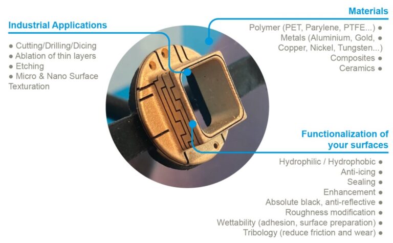
- Cutting, Drilling, Dicing
- Decoating
- Etching
- Micro- and nano-texturing of surfaces (LIPSS, DLIP, biomimetic superhydrophobicity)
Matériaux traités
Polymers (PET, Parylene, PTFE), metals (aluminium, gold, copper, nickel, tungsten), composites, céramiques.
Obtainable surface functionalizations
Hydrophilic/hydrophobic, anti-icing, waterproofing, cosmetic enhancement, non-reflective jet black, surface roughness modification, wettability (adhesion, surface preparation), tribology (reduction of friction and wear).
HEF laser abilities in numbers
- 10 femtosecond laser sources up to 300 W
- 2 complementary laser sources
- 13 laser platforms in production
- 2 6-axis robots
- 1 mobile industrial demonstrator
- 1 additive manufacturing machine
- 6 work surfaces up to 600 x 800 mm
HEF value chain
Vertical integration of R&D into production: technical specifications, science and research, engineering and design, equipment manufacturing, surface treatment, and the manufacture of components incorporating our technologies.
How does femtosecond laser engraving work?
Ultra-fast laser technology enables precision engraving with high machining speeds (mm³/s) and a surface roughness of less than a µm without damaging the material in 2D or in 3D.
Femtosecond lasers enable engraving with thermal control and minimal material damage for applications such as microchannel fabrication, tribology, waterproofing, aesthetics and more.

View technical details (femtosecond engraving)
Femtosecond laser etching
Femtosecond technology allows for precision etching with high machining rates (mm³/s) and a surface roughness of less than 1 µm, without damaging the material in 2D and 3D applications, which is essential for precision industries.
Typical applications
- Microchannel creation
- Tribology (reduction of friction and wear)
- Sealing
- Aesthetics and optical functionalization
- 3D interconnection circuits via successive layer ablation
Compatible PVD coatings
Gold, silver, titanium, aluminum, chromium, carbide.
Key benefits
- No thermal alteration of the substrate
- Extreme precision, thermal control
- Preservation of material integrity
Application Sectors
Energy, aerospace, optics, electronics, medical, consumer goods.
How does femtosecond laser texturing alter surfaces?
Ultrafast laser surface texturing allows for the structural properties of the material to be modified in order to bring technical functionality to the component.
Laser technology enables texturing via high-speed ablation (mm³/s) at very high resolution (µm) without damaging the material, in both 2D and 3D.
Femtosecond lasers also allow for the creation of nanoscale surfaces for various functionalities:
- Wettability (hydrophobic, hydrophilic, etc.)
- Waterproofing
- Anti-icing
- Tribology (friction, grip, adhesion, etc.)
- Conductivity
- Coloration (absolute black, iridescent effect, etc.)

View technical details (femtosecond surface texturing)
Femtosecond laser surface texturing
Femtosecond technology allows for high-speed texturing through ablation (mm³/s) at very high resolution (µm) without damaging the material in 2D and 3D. Texturing creates micro- and nanoscale structures within the material to modify its functional properties.
Obtainable nanoscale surfaces
- Chemical catalysis
- Light reflection (absolute black, iridescent effect)
- Tribology (reduction of friction and wear)
- LIPSS sutructures (Laser-Induced Periodic Surface Structures)
- DLIP textures (Direct Laser Interference Patterning)
- Biomimetic superhydrophobicity (lotus effect)
Surface functionalization
- Hydrophilic or hydrophobic (wettability)
- Self-cleaning
- Cosmetic enhancement
- Enhanced adhesion
- Solder preparation
Types of treated glass
Gorilla Glass, aluminosilicate, borosilicate, fused silica, Lotus XNT.
Additional HEF treatments
Precision polishing, etching, surface finishing.
Industries
Energy, aerospace, optics, electronics, luxury goods, transportation.
How precise is femtosecond laser cutting and drilling?
Laser drilling enables the creation of small holes (up to 10 µm in diameter) with various geometries, for applications on glass, metals, and plastics.
Laser technology allows for through-cutting on various materials (≤ 1 mm thick) at high speeds (1 m/s in a straight line and ≥ 0.2 m/s for more complex geometries).
Laser cutting preserves the substrate by controlling thermal effects and producing clean, burr-free cut edges.

View technical details (femtosecond cutting and drilling)
Femtosecond cutting
Femtosecond technology enables high-speed through-cutting of various materials (thickness ≤ 1 mm): 1 m/s in a straight line and ≥ 0.2 m/s for complex geometries. Essential for cutting applications on glass, metals, and plastics.
Compatible Materials
All materials, from the hardest to the most fragile: biological tissues, polymers, thin metals, and technical glasses.
Flagship application: bipolar plates for fuel cells
- Substrates: graphite, titanium, stainless steel, nickel
- HEF CERTESS® Elec (PVD) coating for modifying electrical properties
- Benefits: thermal control, fine cutting without burrs
Laser drilling
Small holes (up to 10 µm in diameter) with various geometries, suitable for use on glass, metals, and plastics.
Key benefits
- Athermal process (preserves the substrate)
- Precise cutting with clean, burr-free edges
- Controlled thermal effects
Industries
Energy (hydrogen, fuel cells), aerospace, optics, electronics, medical, and mechanical engineering.
How does selective thin-layer ablation work?
Decoating allows for the selective removal of a layer from its substrate without causing delamination, burrs, or microcracks.
This technique is applicable to both functional coatings and precision marking, without causing thermal damage to the substrate.

View technical details (selective removal of thin layers)
Decoating with femtosecond laser technologies
Femtosecond technology allows for the selective ablation of one or more layers from a multi-material component at high speeds (mm³/s) and very high resolution (< 1 µm). This level of precision is essential for applications in microelectronics, hydrogen, and aerospace.
Technical concept
Laser ablation of thin layers (or decoating) enables the selective etching of a layer from its substrate without delamination, burrs, or microcracks. Precise removal of the metallized layer without affecting the underlying layers.
Typical application: Kapton film
- Substrate: polyamide film (Kapton)
- PVD coatings processed: graphene, gold, copper, aluminum
- Selective removal of the metallized coating
Key benefits
- No thermal damage to the substrate
- Extreme precision (submicron resolution)
- Improved local electrical conductivity
- No delamination, no microcracks
Application Sectors
Hydrogen (PEMFC bipolar plates, electrolyzers), aerospace, optics, electronics, medical, transportation.
Questions fréquentes sur le laser femtoseconde
Qu’est-ce que le laser femtoseconde (ou laser ultra-rapide) ?
Quels matériaux peut-on traiter avec le laser femtoseconde HEF ?
Quelles fonctionnalisations de surface le laser femtoseconde permet-il ?
Dans quels secteurs le laser femtoseconde est-il utilisé ?