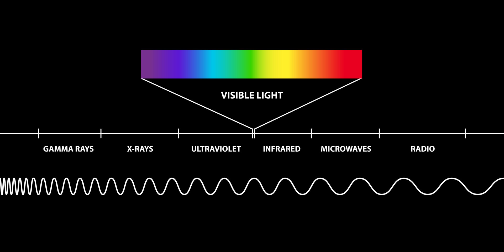
The difference between infrared light and “regular” light lies in their wavelengths. The wavelength of visible light is in the range of several hundred nanometers, while infrared light spans a broader range of wavelengths, from micrometers (near infrared) to millimeters (far infrared). These larger wavelengths compared to visible light have an impact on the sensors. Indeed, the pixels of a device cannot physically be smaller than the wavelength of the radiations they are meant to detect.
This means that the pixels in infrared images are larger, and infrared images are fundamentally less resolved than those produced by optical sensors in the visible spectrum.
An Innovation to Counter Self-Illumination
In addition to the resolution issue, infrared sensors face the well-known problem of self-illumination. Indeed, any warm object (by “warm,” we mean “not at absolute zero”) emits light (think of a heated iron bar whose color changes from red to yellow and then to intense white-blue as its temperature increases).
At ambient temperature, all objects emit… infrared radiation, precisely. This is very useful for detecting human body heat on a battlefield or assessing thermal leaks in a house. However, it also means that the infrared sensor itself (and all the equipment surrounding the sensor) also emits infrared radiation, which, if not controlled, can saturate the sensor and render it ineffective.
To solve this problem, the sensor can be cooled so that it emits very little radiation, allowing it to detect only the infrared radiation coming from external sources. Unfortunately, this cooling process requires additional equipment, which has long hindered the miniaturization of such devices.
Technologies Supporting Progress
New technologies now enable infrared imaging with ever-increasing resolution, thanks to new low-noise pixel types like microbolometers. They even allow for use without cooling, thanks to an electronic processing chain that cleans the signal and significantly improves the signal-to-noise ratio.
But beyond the sensor itself, there is an increasing need for optical components (lenses, prisms, etc.) that also function in the infrared spectrum. These infrared components are made from very specific materials such as semiconductors or chalcogenides and are specifically designed to transmit two specific wavelength bands: those between 3 and 5 microns (used for measuring and controlling the temperature of hot objects remotely, such as in industrial applications) and those between 8 and 12 microns (used for infrared vision systems for human bodies or measuring energy loss in buildings). These two bands are ranges of wavelengths that are either not absorbed or minimally absorbed by the Earth’s atmosphere, making them easy to use.
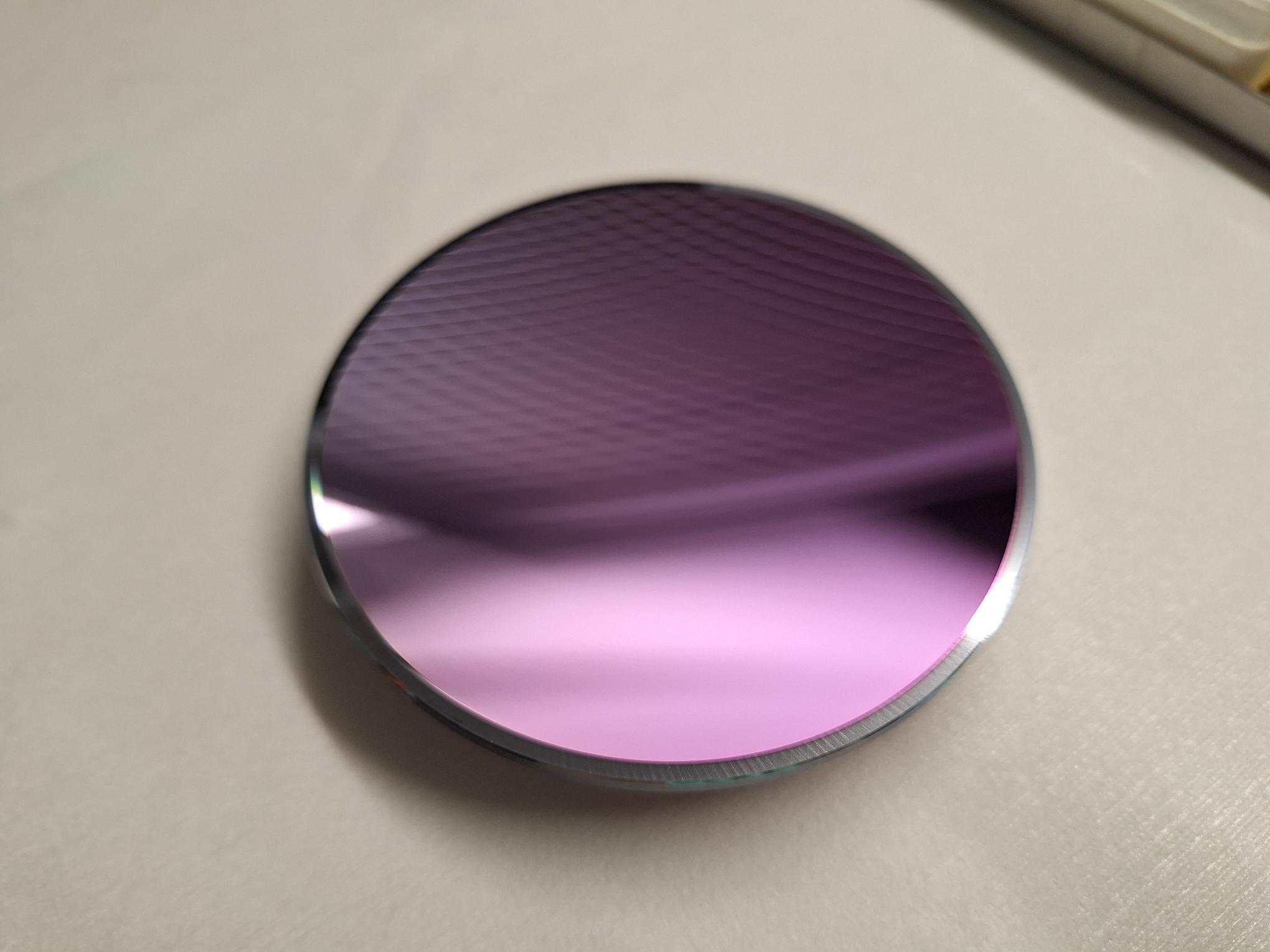
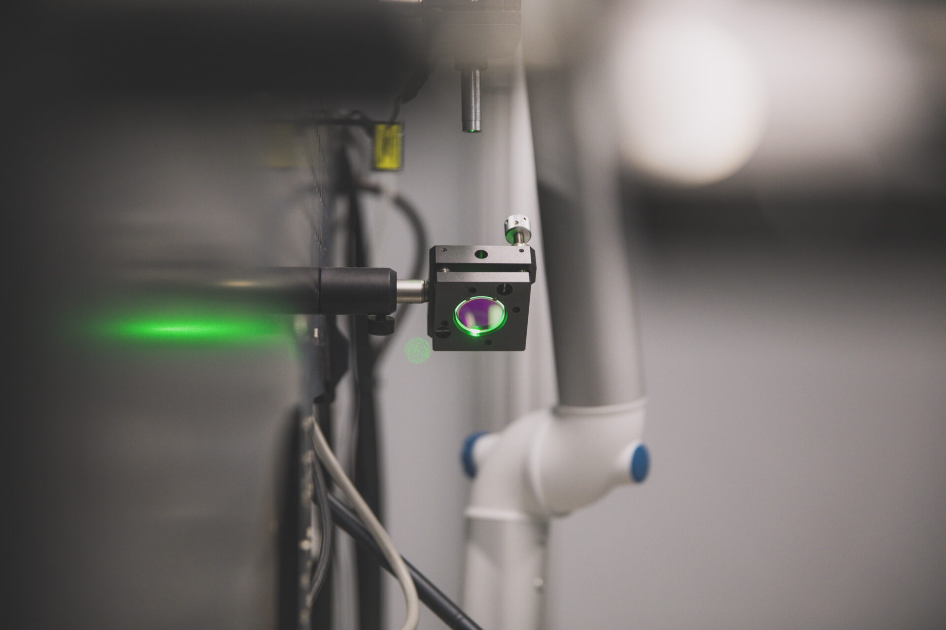
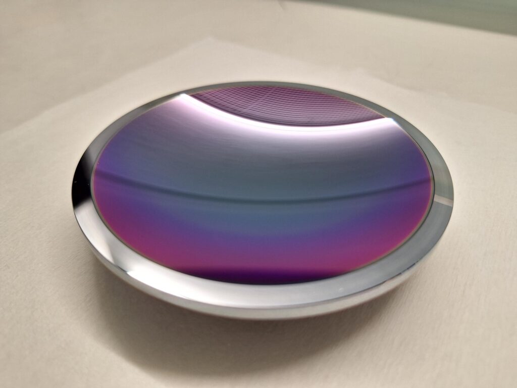
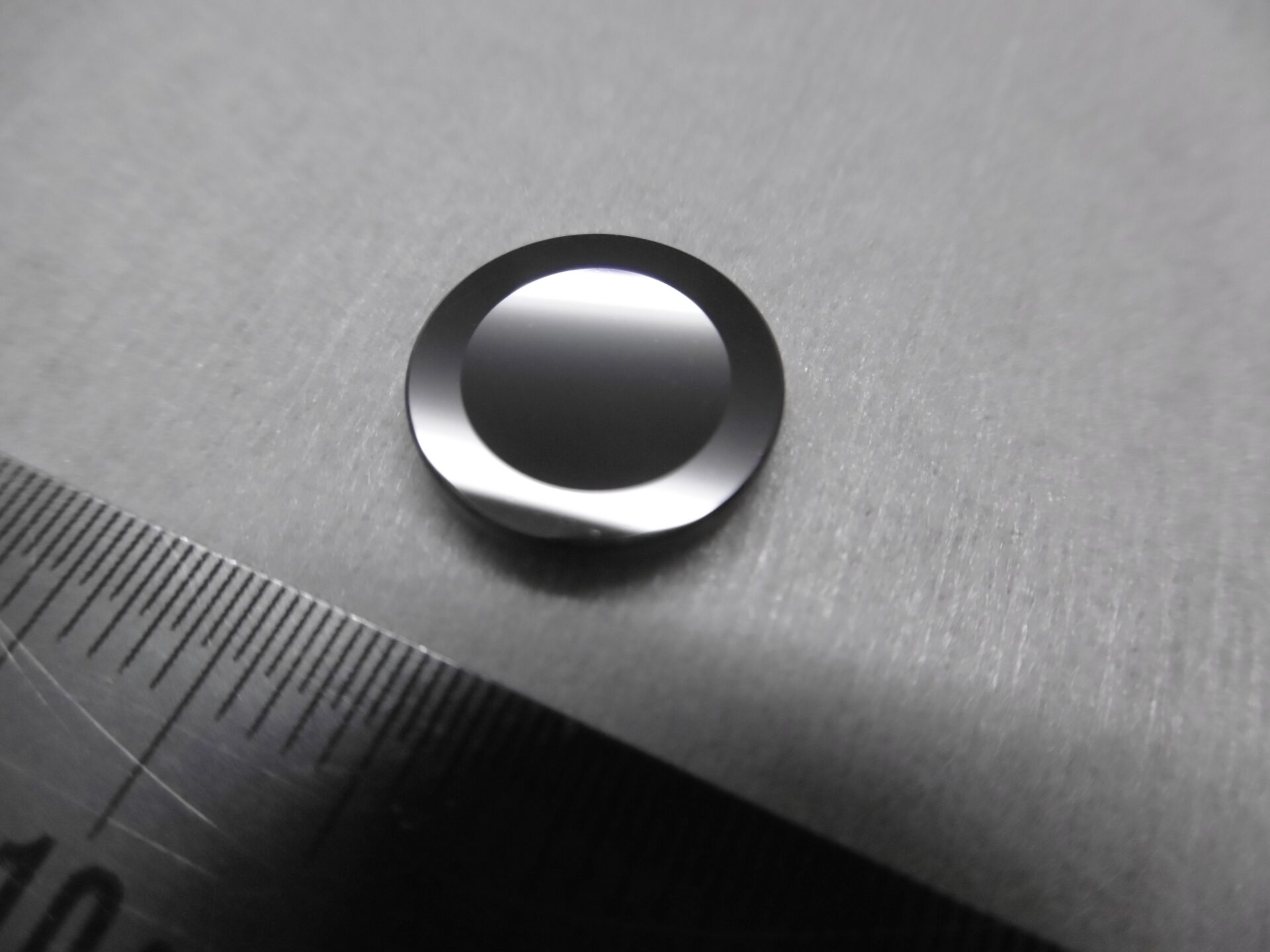
The relatively broad width of these infrared bands requires precise and complex manufacturing processes, which HEF has been developing for years through its HEF PHOTONICS division, mainly at its Lannion site in France. Anti-reflective coatings for optical components used in infrared equipment are more delicate than in visible light. They are applied by alternating more layers and thicker layers.
This optical expertise allows our group to offer tailored surface treatments for infrared optical components for all types of devices, from thermal sensors and infrared cameras developed for civil (thermal examinations, insulation, forest fire surveillance), industrial (automotive, building, electrical cabinet heating), military (night vision goggles), or scientific (biological examinations) applications.
High-Performance Surface Treatments
The surface treatments for optical components in infrared systems offered by HEF are highly demanding. They must provide excellent transparency across the entire chosen spectral band while also protecting the mechanical surface of the optical components.
“All these treatments are carried out by vacuum evaporation with ionic assistance. They are adapted for all types of surfaces (flat, concave, convex) with diameters ranging from 1 to 500 mm. We also combine our optical expertise with ‘hard coating’ treatments, such as carbon coatings (one of the group’s key treatments for tribological applications), which have been adapted to harden and protect the external surfaces of infrared optical components from environmental factors (rain, wind, sand, humidity, etc.).”
Damien Deubel, Director of KERDRY (HEF PHOTONICS subsidiary)